The Sutter-Fella lab is a part of the Lawrence Berkeley National Lab’s Molecular Foundry which is a national User Facility. We are located in Berkeley, California.
Semiconductors are indispensable for mankind, on one hand as building blocks for technical advancement, and on the other hand for energy generation and storage technologies. Research in the Sutter-Fella lab is devoted to formation and characterization of functional semiconductors for applications in optoelectronic devices and energy conversion. We are interested in light-matter interaction, charge transport, structure-function and synthesis-property relationships. We are also working on the development of new experimental probes to promote a sea change in our ability to control matter and energy.
The multidisciplinary research performed bridges chemical engineering, materials science, and physics. It provides insights into the optoelectronic properties of semiconductors through a combination of spectroscopic methods, including synchrotron X-ray techniques, imaging, and electrical measurements.
Our current research focus is on 3D hybrid organic-inorganic metal halide perovskites, perovskite-type oxides, and lead-free double halide perovskites for energy conversion including optoelectronic applications such as photovoltaics, lasers, LEDs, and photocatalytic conversion of CO2. These compounds present great model systems given their rich research challenges and multitude of compositions. We are particularly interested in evolution of properties including crystal phase, luminescence, and morphology under different synthesis conditions. In this regard we are working on multimodal in situ capabilities to enable real time monitoring.
Research examples
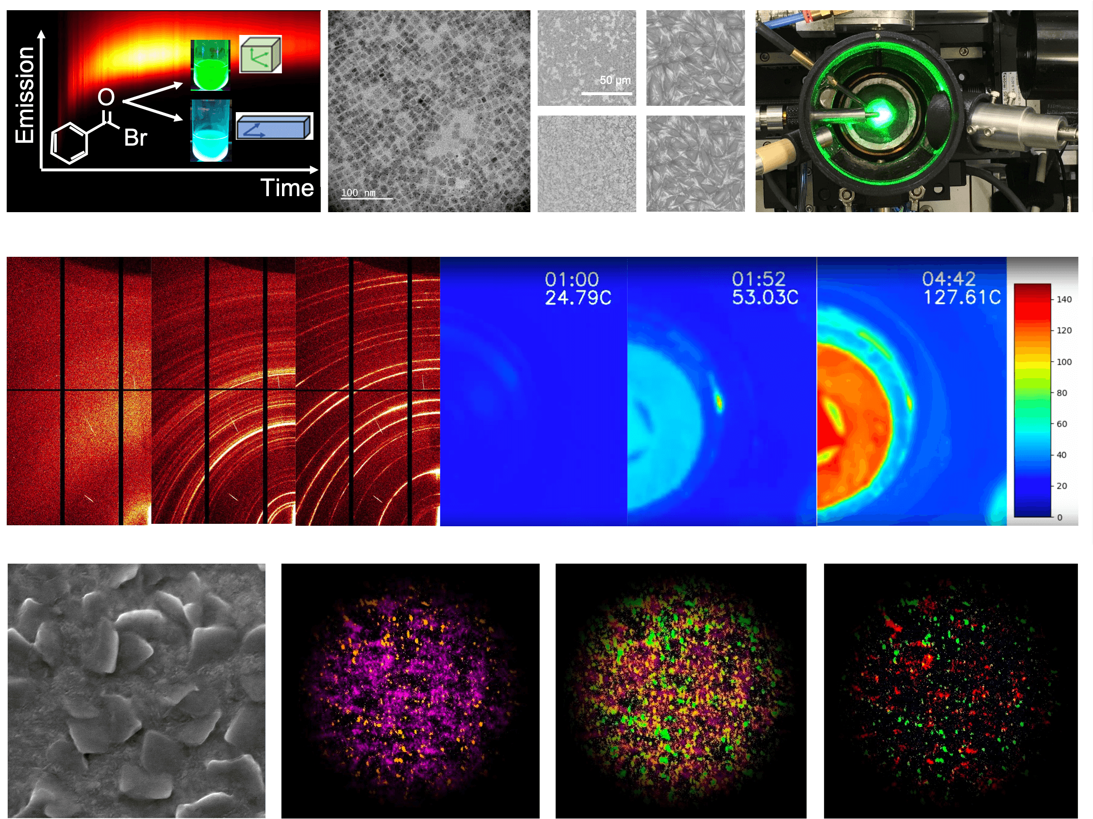
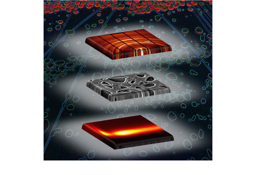
Multimodal in situ characterization during synthesis enables us to reveal formation pathways and evolution of structural as well as functional properties. This knowledge is critical to screen synthetic parameters, discover metastable materials, and ultimately can lead to controlled syntheses that yield high-efficiency devices. Our development of synchrotron- and lab-based multimodal platforms has been recently highlighted as an ALS brief.
Babbe et al., Adv. Energy Mater. (2020)
Song et al., ACS Appl. Energy Mater. (2020)
Song et al., Adv. Funct. Mater. (2019)
Do et al., Nanoscale (2019)
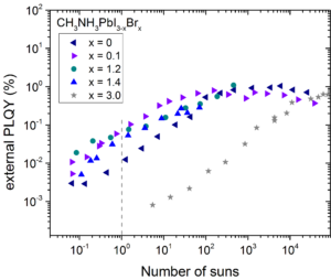
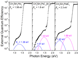
The bandgap of metal halide perovskites can be tuned via halide alloying. Mixed metal halide perovskites offer bandgaps in the visible to the near-infrared range which makes them promising candidates for single junction solar cells as well as top cell in tandem devices. Here we investigate the optoelectronic properties of wide bandgap mixed halide CH3NH3PbI3-xBrx perovskites by pump power dependent photoluminescence quantum yield (PLQY) measurements. Although the PLQY is high, given the fact that these films are hybrid organic-inorganic in nature, there are substantial non-radiative recombination losses at 1-sun illumination. Using very sensitive photocurrent spectroscopy, we measure the sub-bandgap response from bound to free electronic states that generate a photocurrent and find defects in the bandgap that move closer to midgap upon Br-alloying (work in collaboration with the University of Oregon, Prof. Lonergan).
Sutter-Fella et al., Nano Lett. 16, 800-806 (2016)
Sutter-Fella et al., ACS Energy Lett. 2, 709-715 (2017)
Another research area we are interested in is centered around the question why does the open-circuit voltage in mixed halide perovskites does not linearly increase with the increase of the optical bandgap upon substitution of Iodine by Bromine? Understanding illumination induced halide demixing is a critical topic to enable efficient tandem devices employing wide bandgap perovskite based top cells.
Sutter-Fella et al., Nano Lett. 18, 3473–3480 (2018)